Elmar Mitterreiter, Bruno Schuler, Ana Micevic, Daniel Hernangómez-Pérez, Katja Barthelmi, Katherine A. Cochrane, Jonas Kiemle, Florian Sigger, Julian Klein, Edward Wong, Edward S. Barnard, Kenji Watanabe, Takashi Taniguchi, Michael Lorke, Frank Jahnke, Johnathan J. Finley, Adam M. Schwartzberg, Diana Y. Qiu, Sivan Refaely-Abramson, Alexander W. Holleitner, Alexander Weber-Bargioni & Christoph Kastl
Nature Communications 12, 3822 (2021)
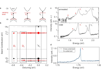
For two-dimensional (2D) layered semiconductors, control over atomic defects and understanding of their electronic and optical functionality represent major challenges towards developing a mature semiconductor technology using such materials. Here, we correlate generation, optical spectroscopy, atomic resolution imaging, and ab initio theory of chalcogen vacancies in monolayer MoS2. Chalcogen vacancies are selectively generated by in-vacuo annealing, but also focused ion beam exposure. The defect generation rate, atomic imaging and the optical signatures support this claim. We discriminate the narrow linewidth photoluminescence signatures of vacancies, resulting predominantly from localized defect orbitals, from broad luminescence features in the same spectral range, resulting from adsorbates. Vacancies can be patterned with a precision below 10 nm by ion beams, show single photon emission, and open the possibility for advanced defect engineering of 2D semiconductors at the ultimate scale.

![[Translate to English:]](/fileadmin/user_upload/sites/bccms/images/logos/bccms-logo-2022-subline-padded-up.png)
