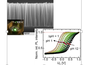
Semiconductor nanostructures exhibit a large surface to volume ratio that makes their electronic structure being strongly dependent on surface processes such as adsorption of molecules or charges in gaseous and liquid environments. Due to their efficient photoluminescence (PL) emission group III-nitride nanowires and nanowire heterostructures sensitively respond to such processes, thus presenting a powerful platform for the realization of optochemical sensors. In addition to the possibility of detecting oxidizing and reducing gases in gaseous ambients or of ions in liquids, optically activated charge transfer to molecules or redox couples provides the possibility of monitoring chemical surface processes occurring on the nanowire surface. We demonstrate such applications and discuss the underlying detections mechanisms in gaseous and liquid envirnments.
Martin Eickhoff is the head of the research group Solid State Materials at the Institute of Solid State Physics, University of Bremen. In his work he focuses on growth and characterization of wide band gap semiconductors and their hetero- and nanostructures as well as novel quantum materials for the application in chemical sensors, biochemical sensors, optoelectronics and nanophotonics.

![[Translate to English:] Zur Startseite des KKBS](/fileadmin/user_upload/fachbereiche/fb3/kksb/logo/KKSBSchriftMitLogoSchwarz_90.png)

