Facilities
Cleanrooms
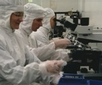
IMSAS uses a variety of facilities for research, development and production of state-of-the-art microsystems. Two large class ISO 6 cleanrooms with an overall area of 900 m² for front-end and back-end processing of 100 mm and 150 mm wafers are available, offering the complete range of standard MEMS processes:
Photolithography
- Contact-Lithography
- Laser-Lithography
- 3D-Lithography
Thermal Processing
- Oxidation
- Diffusion
- Annealing
- Parylene Coating
Deposition
- Low Pressure Chemical Vapour Deposition
- Low pressure chemical vapor deposition (LPCVD)
- Plasma Enhanced Chemical Vapor Deposition (PECVD)
- Sputtering
- Evaporation
Etching
- Wet Etching
- Reactive Ion Etching (RIE)
- Deep Reactive Ion Etching (DRIE) / Advanced Silicon Etching (ASE)
- Ion Milling Etching
- Plasma etching (PE)
Electro Plating
Waferbonding
- Silicon Fusion Bonding (SFB)
- Anodic Bonding
- Eutectic Bonding
- Solder Bonding
- Glass-Frit Bonding
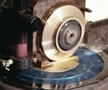
Chemisch-Mechanisches Polieren (CMP)
Assembly and Packaging Technology
IMSAS has a great variety of specialised equipment to enable assembly and packaging technology at the ende of the MEMS production:
- Waferdicing
- Chipbonding
- Wirebonding
- (PCB) Processing
Test and Characterizing
For fabrication as well as for testing and characterization of MEMS (Micorelectromechanical Systems) devices IMSAS has a multitude of measuring instruments and stations:
- Film-Thickness Measurement Tools
- Step Height Prober
- Surface Profiler
- 3D Measurement System
- Gauge for film stress
- 4-Point Resistivity Prober
- Scanning Electron Microscope (SEM)
- X-Ray Fluorescence Spectrometer
- Pressure Measuring Station
- Flow Measuring Station
- Gas Measuring Station
- Climatic Exposure Test Cabinet
- Impedance spectroskopy
Design und Simulation
Numerous design and simulation tools enable IMSAS to create and optimize MEMS designs in-house:
- CoventorWare®
- LabVIEW®
- MATLAB®
- COMSOL Multiphysics®


