Abstract and Intermediate Report
ABSTRACT
In order to successfully conclude my thesis supervised by Dr. J. C. Nolasco and Dr. A. Castro-Carranza with outstanding results, the general goal of this short research stay at Prof. Gutowski’s Semiconductor Optics research group, Institute of Solid State Physics, is to carry out optical and electrical characterization of samples based on CuO and ZnO deposited on indium tin oxide (ITO) substrates for solar cell applications. All the studied samples have been fabricated in Mexico and they consist of: (i) heterojunctions formed by PCBM/CuO bilayers and contacted by Ag electrodes; and (ii) ZnO nanowires grown by wet-chemical deposition. Additionally, thin films of polystyrene have been deposited on some samples as interlayers to analyze the charge recombination rate at the heterojunction interface in our solar cell architectures. By applying optical and electrical characterization techniques, i.e, photoluminescence spectroscopy, photoconductivity, current-voltage and impedance spectroscopy, and circuit modeling, we aim to extract both the density of defect states and information about the charge transport mechanisms within the devices with different architectures. Once identifying the losses, we will define the optimal technological parameters to fabricate efficient low-cost solar cells based on these materials.
INTERMEDIATE MAPEX REPORT
Starting on September 9, 2019, I have been hosted by the Semiconductor Optics research group led by Prof. Dr. Jürgen Gutowski, Institute of Solid State Physics, Faculty of Physics and Electrical Engineering, University of Bremen, Germany, given the close cooperation between this group and my thesis supervisors Dr. Jairo C. Nolasco and Dr. Alejandra Castro-Carranza who is also Research Ambassador of the University of Bremen for Mexico.
The general goal of this short research stay has been to carry out optical and electrical characterization of samples based on CuO deposited on indium tin oxide (ITO) substrates for solar cell applications, that is complementing our research performed at ENES Morelia UNAM. The samples were fabricated in Mexico using a sustainable and low-cost chemical bath method, and they consist of heterojunctions formed by PCBM/CuO bilayers on ITO and contacted by Ag electrodes. Additionally, ZnO nanowire samples grown on ITO by wet-chemical deposition were fabricated in order to compare the performance of both types of devices. To tune the properties of the heterojunction's interface, besides modifying the CuO and ZnO chemical bath deposition parameters, some samples have been passivated by thin films of polystyrene as interlayers to avoid recombination in solar cell architectures.
Up to now, the following activities have been carried out:
- Preparation of the setup to measure impedance spectroscopy
- Electrical characterization of solar cells based on ZnO
- Thickness measurements of the CuO samples using profilometry in an atomic force microscope.
- Micro-photoluminescence characterization of CuO and ZnO samples
With these activities we have initiated the extraction of the defect density of states in our samples, and have obtained evidence that the passivation of the heterojunctions plays an important role to decrease recombination within the devices, and therefore to improve the efficiency of the solar cells.
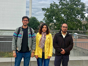
Discussions of the results obtained in Bremen and Morelia have generated a fruitful environment with members of the Semiconductor Optics group, specifically with Prof. Dr. Gutowski, Dr. Alexander Kothe and M. Sc. Wilken Seemann who have supervised the activities in the laboratories. As for the Mexican part contributing to the discussions and results, besides Dr. Nolasco, the student Andres Castro Chacón co-funded by UNAM, Mexico, has been part of this enriching experience. In addition, I would like to mention that we are the first students of ENES Morelia UNAM coming to the University of Bremen in the framework of the cooperation agreement (CM-CSAM-UJ-CV-I-06-026/2018) signed in November 2018 by directives of the Faculty of Physics and Electrical Engineering (FB1) and ENES Morelia UNAM. . I hope that my stay here can foster an intensive collaboration between both Universities, including the mobility of more students in the near future.
I gratefully thank the University of Bremen and the MAPEX Center for Materials and Processes for giving me the opportunity to carry out this research stay that is adding a great value to my professional and personal development.


