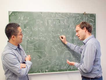
Scientists at the University of Bremen are investigating new mechanisms for the targeted alteration of the conductivity of nanomaterials. They recently published their discovery in the internationally renowned journal “Nature Communications.”
For some years now, it has been possible to produce ultrathin materials that are only a few atoms “thick.” Probably the best researched of these two-dimensional (2-D) materials is graphene, an atomic layer of carbon atoms. Groundbreaking experiments on graphene were awarded the Nobel Prize in physics in 2010. In addition to graphene, other atomically thin materials such as drilling nitride or so-called transition metal dichalcogenides such as TaS2, which the physicists in Bremen have investigated, can also be produced. In contrast to ordinary volume materials, practically all atoms of these 2-D materials are located directly on the surface. Scientists hope that this will open up completely new possibilities for tailoring material properties.
Tracking Down Nanomaterials of the Future
An international team of researchers from the universities of Bremen, Aarhus, and Nijmegen has now achieved a breakthrough in this field. As they report in the journal “Nature Communications,” the team around Professor Tim Wehling and Dr. Bin Shao from the Institut für Theoretische Physik and Bremen Center for Computational Materials Science at the University of Bremen has discovered a new mechanism for introducing electrons into ultrathin materials. This trick could make it possible to develop new nanomaterials for information and energy technology.
Avoiding the Disorder Problem for 2-D Materials
The introduction of moving charge carriers into electronic materials, also known as doping, is an important way of manipulating materials. It forms the basis of today’s entire semiconductor-based information processing or photovoltaics. In classical semiconductors such as silicon, doping works by replacing individual atoms. “In order to be able to use ultrathin 2-D materials for applications, it is important to dope them,” explains Professor Tim Wehling. However, because 2-D materials are so thin, the electrons are strongly disturbed by the introduction of foreign atoms. Due to these so-called disorder effects, desirable properties such as high conductivities are often lost. “The doping mechanism discovered now avoids the disorder problem for 2-D materials by exploiting the fact that electrons can be quantum mechanically in several places at the same time. Foreign atoms are no longer needed for doping. Instead, the electrons constantly tunnel into and out of the 2-D material from their environment,” Wehling continues.
New Method Enables Highly Sought-after Superconductivity
For today’s applications in semiconductor technology, significantly less than one electron per 1,000 material atoms is moved. The new method now allows doping that is more than a hundred times stronger. This can lead to a fundamental change in the behavior of the electrons. Effects such as superconductivity (i.e. the flow of electric currents without energy loss) and so-called charge density waves (an electronic analog of water waves) can be influenced.
Basis for a Wide Range of Applications
According to Wehling, the work now published first describes basic research on the material system of tantalum disulfide (TaS2) on a gold surface. “However, the doping mechanism discovered should also work more generally for metallic 2-D materials and thus be able to find broad technical application in the long term,” he hopes. The next step is to understand how this effect can be exploited to manipulate electronic properties of 2-D materials, especially superconductivity and charge density waves. The latter are in the focus of intensive research efforts in the context of novel information processing concepts as possible components of artificial neural networks. The same applies to the field of superconductivity, where new materials could enable applications in the field of virtually loss-free power transport or particularly efficient electric motors.
The article “Pseudodoping of a metallic two-dimensional material by the supporting substrate” can be found at www.nature.com/articles/s41467-018-08088-8 (DOI number: doi.org/10.1038/s41467-018-08088-8 ).
Additional Information:
www.itp.uni-bremen.de/ag-gies
www.uni-bremen.de
Contact:
Professor Tim Wehling
Institut für Theoretische Physik and Bremen Center for Computational Materials Science
University of Bremen
Tel.: +49 421 218-62039
E-mail: twehlingprotect me ?!uni-bremenprotect me ?!.de


