Christian Tessarek; Tim Grieb; Christian Petersen; Alexander Karg; Niels Osterloh; Christian Habben; Stephan Figge; Jon-Olaf Krisponeit ; Thomas Schmidt; FaltaJens; AndreasRosenauer; Martin Eickhoff
2D Materials 11 (2024): 025031
doi: https://doi.org/ 10.1088/2053-1583/ad3134
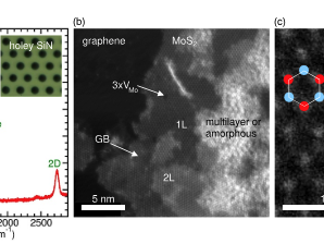
MoS2 and WS2 mono- and multilayers were grown on SiO2 /Si substrates. Growth by atomic layer deposition (ALD) at fast growth rates is compared to sub-ALD, which is a slow growth rate process with only partial precursor surface coverage per cycle. A Raman spectroscopic analysis of the intensity and frequency difference of the modes reveals different stages of growth from partial to full surface layer coverage followed by layer-by-layer formation. The initial layer thickness and structural quality strongly depend on the growth rate and monolayers only form using sub-ALD. Optical activity is demonstrated by photoluminescence (PL) characterization which shows typical excitonic emission from MoS2 and WS2 monolayers. A chemical analysis confirming the stoichiometry of MoS2 is performed by x-ray photoelectron spectroscopy. The surface morphology of layers grown with different growth rates is studied by atomic force microscopy. Plan-view transmission electron microscopy analysis of MoS2 directly grown on freestanding graphene reveals the local crystalline quality of the layers, in agreement with Raman and PL results.
© 2024 IOP Publishing Ltd.


