


© 2025 The Author(s). Published by IOP Publishing Ltd.
Spectroscopy|
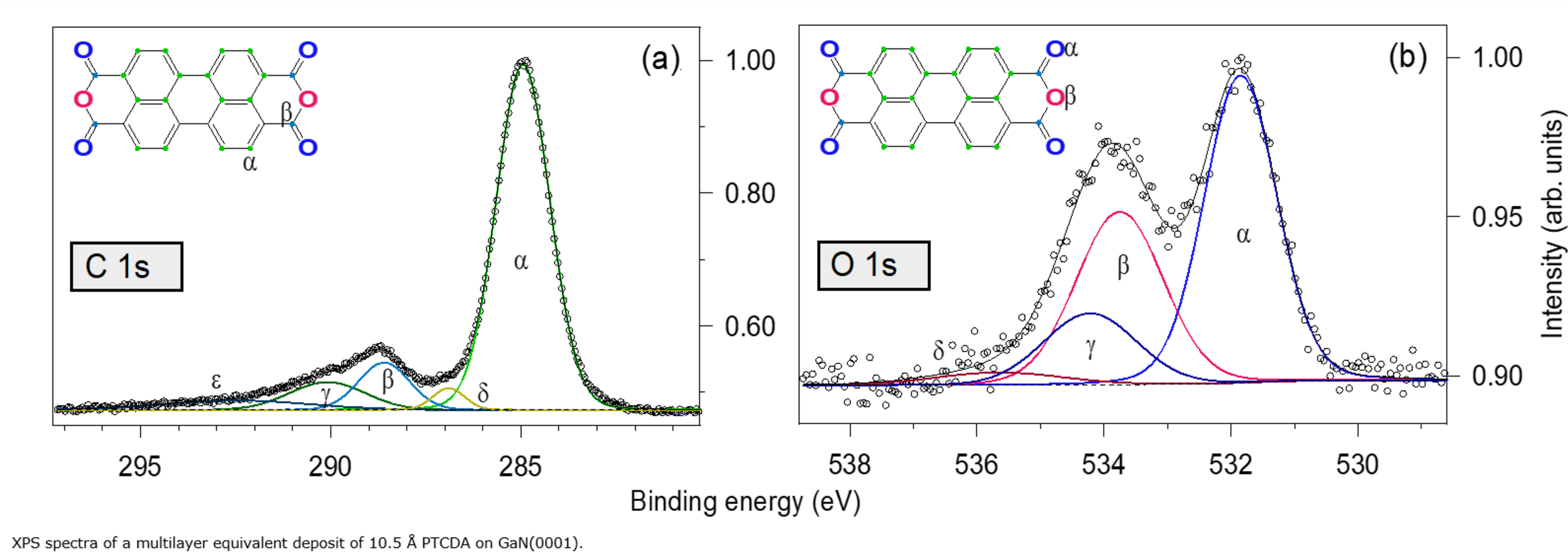
The kinetic energy of electrons emitted from atomic core levels after x-ray photo absorption is characteristic of the respective element and its chemical state, giving rise to individual spectral lines which can be used, e.g., to distinguish different oxidation states with XPS. Combined chemical and structural information are contained in so-called LEEM-IV measurements, where, in a separate experimental setup, low-energy electron reflectivity is recorded as a function of the incident electron energy. Such chemical and structural surface phases can be identified with a lateral resolution of a few tens of micrometers.
Complementary, the vibrational and structural properties of samples can be investigated using Raman and circular dichroism spectroscopy setups.
With XPS and LEEM both the chemical composition as well as the local structure and morphology of samples can be addressed. Since both techniques employ electrons with rather low energy, the information depth is restricted to a few atomic layers, and a decent electrical conductivity of the samples is required as well as ultra-high vacuum compatibility. Spectra and images can also be taken at elevated temperatures as well as during gas dosing (up to 10-4mbar) to study changes of the chemistry, structure, and morphology during annealing or interaction with gases.
The local bonding geometry can be revealed with vibrational (Raman) spectroscopy. Circular dichroism spectroscopy (CDS) allows for the investigation of chiral structures, e.g biomolecules adsorbed at interfaces. Both methods, Raman and CDS, are less surface sensitive than the electron-based methods of XPS and LEEM, and can be obtained from a wider class of specimens (e.g. insulators, non-UHV compatible materials.)
Dr. Jon-Olaf Krisponeit
University of Bremen
Institute of Solid State Physics
Otto-Hahn-Allee 1, D-28359 Bremen
E-mail: krisponeitprotect me ?!ifp.uni-bremenprotect me ?!.de
Dr. M. Mangir Murshed
University of Bremen
Institute of Inorganic Chemistry and Crystallography
Leobener Straße 7, D-28359 Bremen
E-mail: murshedprotect me ?!uni-bremenprotect me ?!.de

Omicron DAR 400 + EA 125
X-ray photoemission spectrometer

SPE-LEEM Elmitec
Spectroscopic low-energy electron microscope

Horiba LabRAM Aramis
Raman Spectrometer

Applied Photophysics Chirascan
Circular dichroism spectrometer


![[Translate to English:]](/fileadmin/_processed_/8/0/csm_FaltaFlege2022_4x3b_0cf8ee65c1.png "[Translate to English:]")
![[Translate to English:]](/fileadmin/_processed_/f/0/csm_Falta2022_4x3_ee7222b4e1.png "[Translate to English:]")
![[Translate to English:]](/fileadmin/_processed_/a/0/csm_Open_Ceramics_2022_MurshedMaas_ae36406658.jpg "[Translate to English:]")
![[Translate to English:]](/fileadmin/_processed_/3/c/csm_MurshedGesing2018_f5f58b2fa6.png "[Translate to English:]")
![[Translate to English:]](/fileadmin/_processed_/6/8/csm_2021_Gogolin_et_al._337b667599.jpg "[Translate to English:]")
![[Translate to English:]](/fileadmin/_processed_/1/2/csm_JPCC_FaltaJOK_2021_2703f1ec1d.gif "[Translate to English:]")


![[Translate to English:]](/fileadmin/_processed_/c/5/csm_Crystal_structure_of_KLi2Ho_BO3_2_931e321e37.jpeg "[Translate to English:]")
![[Translate to English:]](/fileadmin/_processed_/1/4/csm_2020_Schmidt_et_al._ebc9cd99f1.jpg "[Translate to English:]")
![[Translate to English:]](/fileadmin/_processed_/7/d/csm_2019_Stapelfeldt_et_al._f1752c4a67.jpg "[Translate to English:]")

