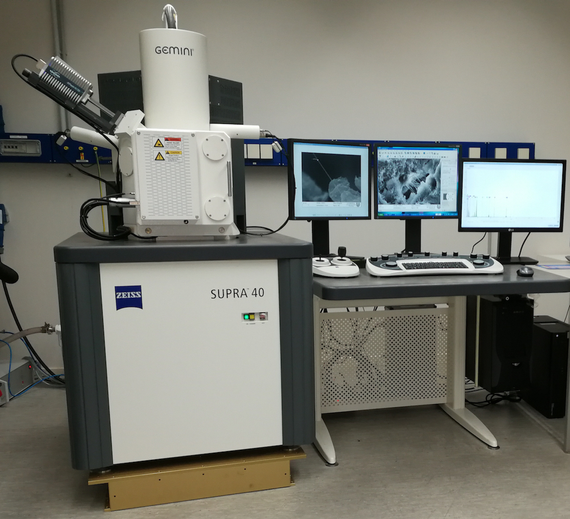
...stands for field emission scanning electron microscopy and energy dispersive X-ray spectroscopy.
FESEM & EDX
How it works
Using Scanning Electron Microscopy, the sample is screened by a fine focussed electron beam. While the sample surface is scanned by the electron beam, an interaction with the sample occurs and electrons with different energy levels are released. These electrons are detected (SE2 / Inlens / BSD / EDS) and result in data about the topography and material composition of the sample.
The most important advantages in comparison to light/optical microscopy are:
- higher resolution
- image sharpness
- relatively simple preparation
- ease of image interpretation due to three-dimensional effect
- use of different contrast mechanisms for the image generation/production
- relatively simple adaption and activation of additional measurement devices in fine-scale analysis
The device
In the Geoscience Department of the University of Bremen, we provide a Zeiss field emission electron microscope SUPRA 40 and a Bruker EDS detector XFlash 6|30 in our lab.
The SUPRA 40 is configured with the newest electron optics which leads to very good results especially for low potential voltage applications. Furthermore, the Inlens-Detector with its high detection efficiency allows the imaging of nanoparticles as small as 15 nm.
Our Silicon Drift Detector (EDS detector) XFlash 6|30 has got an active surface of 30 mm2 and an energy resolution of <129 eV at Mn-Kα. Due to high pulse rates, single point analysis, area analysis, as well as linear analysis (line scan) and element mapping is possible within a very short measurement time.
Sample types
- max. thickness of sample: 30 mm
- max. diameter of sample: 50 mm
- generally it is recommended to prepare the sample as small and flat as possible
- powder samples are possible
- non-conductive samples will be coated in our Cressington Sputter Coater or Carbon Coater to ensure sample conductivity
Furthermore, samples must have the following attributes:
- high vacuum resistance
- dry
- no gas emissions of sample

